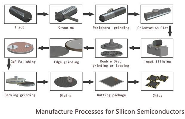
afers are the basic raw materials for the production of semiconductor devices. High-purity semiconductor materials are made into wafers through processes such as crystal pulling and slicing. Wafers produce tiny control circuit structures through a series of semiconductor manufacturing processes, and then through dicing , packaging, and testing become chips, which are widely used in various electronic instruments.
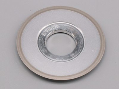
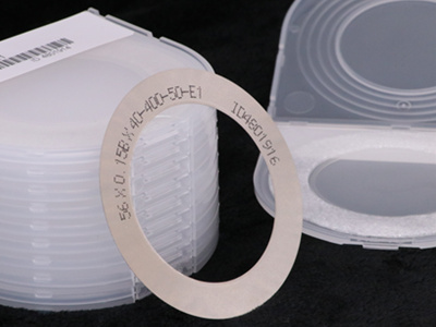
Wafer chamfering and edge chamfering are usually made of curved dicing or internal dicing saw blades. The outer edges of the dicing wafers are particularly sharp. In order to prevent the cracking of the corners from affecting the hardness of the wafer, or damaging the surface finish and subsequent processes bringing environmental pollution, it is necessary to automatically correct the edge, shape and outer diameter of the wafer with special numerical control equipment, so the dicing knife directly affects the quality of the finished product.
Semiconductor wafer dicing machine
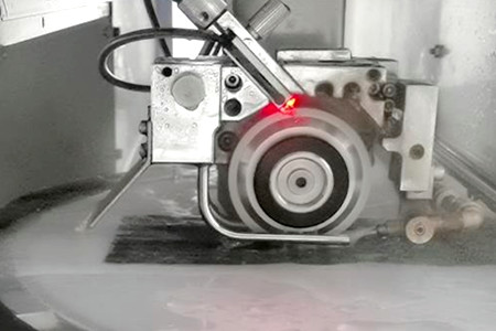
The semiconductor wafer dicing machine divides the wafer containing many chips into wafer particles. The quality and efficiency of dicing directly affect the quality and production cost of chips. Semiconductor wafer dicing machine mainly includes grinding wheel dicing machine and laser dicing machine. Grinding wheel dicing machine is a precision numerical control equipment that integrates technologies such as water, gas, electricity, air static pressure high-speed spindle, precision mechanical transmission, sensors and automatic control. It is characterized by low dicing cost and high efficiency, and is suitable for dicing thicker wafers.
Laser Scribing Machine
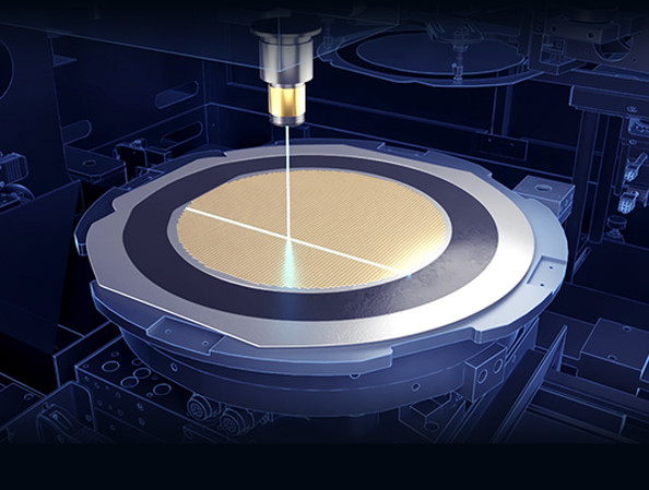
The laser scribing machine uses a high-energy laser beam to irradiate the surface of the workpiece, so that the irradiated area is partially melted and vaporized, so as to achieve the purpose of scribing. It is characterized by high dicing precision and fast dicing speed, and is suitable for dicing thinner wafers.
Dicing/scribing process
Scribing blade dicing methods include one-time dicing and step-by-step continuous dicing. High efficiency, low cost and long service life. It is the most widely used dicing process and has advantages on thicker wafers (>100 microns).
Laser dicing has high precision and high speed. It is mainly suitable for dicing thinner wafers. Diamond dicing is the mainstream dicing technology. dicing uses a blade composed of diamond particles and a binder. During the dicing process, diamond particles are fixed on the tool body with metal nickel as abrasive particles. The blade rotates and feeds at a certain speed, and uses water as the dicing fluid. During the dicing process, the diamond particles expand and form structures called "chip pockets" with the binder, scooping up the dicing channel material and then separating it. During the dicing process, the diamond particles are constantly worn away, exposing new particles, keeping the blade sharp and removing dicing debris. The debris generated during the dicing process will adhere to the blade, so try to prevent the dicing debris from adhering during the dicing process, and properly handle the dicing debris to ensure the normal operation of the blade during the dicing process.
For diamond dicing saw blade, the larger the diamond particles, the stronger the cutting ability of the blade, the slower the wear of the diamond particles, and the longer the service life of the blade. However, the larger the particle size, the greater the impact of the cutting process on the cutting surface, which is likely to cause serious defects such as cracks and chipping. Smaller diamond grits reduce the impact on the cutting surface during cutting and reduce the risk of larger cutting defects. However, if the diamond cannot be shed and renewed in time, it is easy to wrap the cutter, resulting in a sharp decline in the cutting ability of the blade and serious defects.
The diamond particle concentration of the dicing blade body will significantly affect the quality of cutting chips. When the concentration of diamond particles is large, the diamond particles will fall off and be renewed in time with the wear of the binder, which is beneficial to prolong the service life of the blade. Also, the softer the binder, the easier it is for the diamonds to come off, and vice versa. Therefore, cutting with a harder bond can severely damage the cut surface, while a softer bond has less impact and less damage. The choice of diamond particle size and concentration should be combined with the type of binder and should be considered comprehensively.
Dicing process
The chip is cut into individual particles by the wafer, and then it is ready to use after being packaged by the chip. When scribing, the moving speed of the scribing knife and the rotation speed of the scribing knife should be controlled. The thickness of different chips and the viscosity of the blue film need to have corresponding matching parameters to reduce debris during the scribing process. Residual silicon dross from the cutting process can damage cutting tools and swarf, resulting in yield loss. During the cutting process, it needs to be washed with clean water to remove silicon slag, and the spray angle and water volume should be controlled.
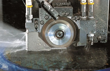
Diamond saw blades dicing wafer blocks at a high speed of 30,000-40,000 revolutions per minute. At the same time, the workbench carrying the wafer moves linearly at a certain speed along the tangent direction of the contact point between the blade and the wafer, and the silicon wafers produced by cutting the wafer are washed away by the separator water. To achieve exceptional chip surface protection during scribing, some chips need to be cut twice in all cuts. At this time, the blade used for the first cut is relatively wide, and the blade used for the second cut is relatively narrow.
Factors Affecting Cut Quality
There are many factors that affect the quality of wafer cutting, including materials, cutting instruments, working environment, cutting methods and other factors. From a material point of view, the silicon substrate and circuit layer materials of the silicon wafer will lead to different mechanical properties during the silicon wafer cutting process. The choice of blades of different materials will have different requirements for the cutting method, and therefore will show different cutting qualities. From the point of view of cutting instruments, since the cutting power of different machines is different, the choice of cutting table will also affect the cutting quality. From the perspective of working environment, the pressure and flow of cooling water are the factors that affect the cutting quality. If the water flow speed is too slow, the cooling effect will be insufficient, and the heat generated by cutting friction will be difficult to discharge and accumulate in time, which may cause the diamond abrasive grains to break, reduce the cutting ability and cutting accuracy of the blade, and affect the cutting of the blade because the cutting debris cannot be removed in time ability. From the perspective of cutting method, it mainly involves cutting depth, blade speed and feed speed. Proper parameters are very important to obtain good cutting quality. Other factors, such as machine operator skill, also affect wafer cut quality.
Dicing defect
The types of defects that are prone to occur in wafer dicing mainly include cracks, chipping and peeling. These defects may cause direct damage to the chip, and may also affect the subsequent packaging and subsequent use reliability of the chip. For example, microcracks generated by dicing will introduce stress into the chip and become a potential chip fragile area, affecting the reliability after packaging. During the cutting process, the chip is impacted by the powerful cutter body, and the metal layer and silicon substrate are peeled off. If the edge collapse is too large, the functional area of the chip will be damaged, which will directly lead to chip failure. The delamination of the metal layer caused by the impact during the cutting process, although the silicon substrate is not damaged, usually does not cause functional damage to the chip, but if the peeling area is large and extends to the functional area, it is also very dangerous.
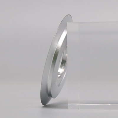
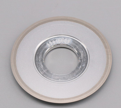
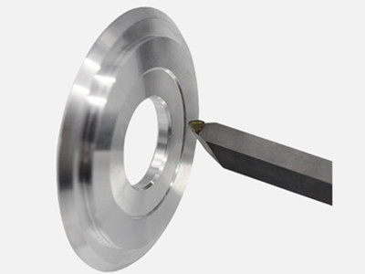
The production of wafer dicing blade is first roughed by carbide tools, then semi-finished by PCD blades, and finally finished by single crystal diamond turning tools to achieve extremely high dimensional accuracy and surface finish.
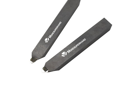
Moresuperhard single crystal turning tool finishes the surface and inner hole of the wafer dicing blade, and the dicing performance is more stable, thereby improving the cutting quality and cutting accuracy of the substrate after the dicing knife is packaged, and greatly increasing the production capacity. It is tailored for users to meet the needs of customers. Its craft and project needs.
Cutting tools for turning diamond dicing blade
Single crystal cutting tools have many advantages in ultra-precision machining. High hardness and wear resistance can minimize the impact of tool tip wear on workpiece size during ultra-precision machining. In addition, good thermal conductivity and low thermal expansion coefficient can prevent large thermal deformation during cutting. Moreover, the surface roughness of the single crystal tool is small, the cutting edge is very sharp, up to Ra0.01-0.006μm, and the single crystal cutting allowance is less than 0.02mm.
Single crystal machinable materials and applicable industries are as follows:
Metal materials: aluminum alloy, aluminum, brass, copper, gold, nickel, silver, tin, zinc, HRC50 hard steel, etc.
Polymer materials: acrylic resin, nylon, polypropylene, polystyrene, silicone, etc.
Infrared crystal materials: calcium fluoride, gallium arsenide, germanium, magnesium fluoride, silicon, zinc selenide, zinc sulfide, etc.
Military industry: off-axis three-mirror, missile fairing, sophisticated infrared optical system, etc.;
Civilian use: spherical, aspheric free-form surface lens, Fresnel lens, high-precision mold core, super-bright and super-uniform light guide plate, compound eye structure, etc.
