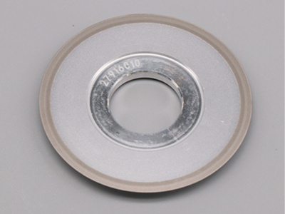
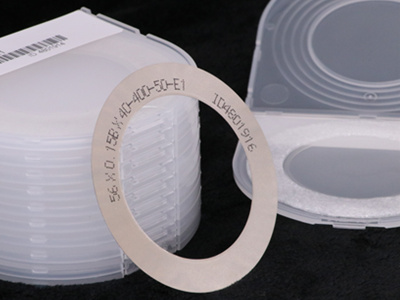
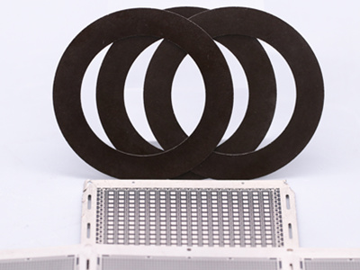
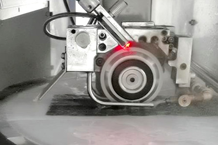
The wafer dicing blade is made of synthetic resin, copper, tin, nickel, etc. as a bonding agent and synthetic diamond. It can be divided into a hub-type diamond dicing blade and hubless diamond blade, which can be used to process chips of different materials and semiconductor-related materials. Therefore, how to choose a suitable scribing blade mainly depends on these factors, such as the particle size and concentration of the diamond, the strength of the blade bond, the length and thickness of the blade, etc.
Moresuperhard can provide:
* Resin diamond dicing blade(Suited for dicing hard and brittle materials,such as QFN, sapphire, quartz and glass, etc)
* Metal diamond dicing blade ( used for cutting and slotting varieties of hard or fragile materials. Such as silicon slices,glass,ferrite,quartz crystals,piezoelectric ceramics,optical glass, FR4, BGA and QFN packages, BGA, magnetic heads, optical sensors , communication, MEC, QFN, etc)
* Electroformed hub dicing blade ( used for cutting Silicon Wafers, copper wafer, IC/LED Packages, Compound Semiconductor Wafers (GaAs, Gap),Oxide Wafers (LiTaO3), Optical Glass)
The effect of diamond particle size on dicing:
1) Large particles: First, the dicing blade edge is large, the removal of debris is large, and the product is not easy to accumulate and precipitate silicon powder; second, the contact surface with the binder is large, it can withstand large resistance, the processing efficiency is high, and it is not easy to wear; the third is with The product contact range is large, the debris and chipping produced are large, and the cutting quality is poor.
2) Small particles: First, the contact range with the product is small, and the debris and cracks produced are small or even no cracks; second, the blade edge is small, the debris removed is small, and the product is easy to deposit silicon powder,the third is the bond with the binder. The contact surface is small, the withstand resistance is small, the processing efficiency is low, and it is easy to wear.
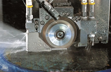
Effect of Diamond Concentration on Dicing Blade
The higher the diamond concentration, the longer the service life of the dicing blade, and the better the chipping angle on the surface, but the worsening the chipping angle on the back side, so the most suitable diamond concentration should be selected according to the demand.
Influence of dicing blade bond strength
1) High-strength binder: first, strong toughness, not easy to break the blade, and high utilization rate; second, strong wear resistance, weak blade regeneration ability, and poor product quality; third, high resistance, slow feed speed, and low efficiency.
2) Low-strength binder: first, small resistance, fast feed speed, and high efficiency. Second, easy to wear, strong blade regeneration ability, and good product quality; third, weak toughness, easy to break the blade, and low utilization rate.
The nickel-based scribing blade for semiconductor cutting uses electroformed nickel-based binder, combined with coarse-grained diamond, to achieve ultra-long life scribing.
4. The effect of particle concentration
1) High concentration: First, there are many cutting edges, more debris removed, and the product is not easy to residue silicon powder; second, the diamond particle load is small, the cutting resistance is small, the progress speed is fast, and the efficiency is high; the third is the small cutting edge of the product, resulting in The debris is small, easy to wash, and the quality is guaranteed; the fourth is less binder, low toughness of the blade, easy to break the blade, and the risk of scratching the product.
2) Low concentration: First, there are more binders, high toughness of the blade, and it is not easy to break the blade; second, there are few cutting edges, less debris removed, and easy silicon powder residue; third, the diamond particle load is large, the cutting resistance is large, and the progress speed Slow and inefficient.
CHICO wafer dicing blade expands the selection range of concentration, which can more accurately meet the various processing needs of users. It can shorten the pre-cutting time and reduce backside cracking.
5. The influence of blade thickness
1) Thickness of the blade: First, the vibration of the blade is small, and the product quality is guaranteed; second, the blade is strong and not easy to break; third, the cutting contact area is large, the resistance is large, the debris generated is large, the feeding speed is slow, and it is easy to pollute.
2) Thin blade: First, the cutting contact area is small, the resistance is small, and the feed speed is fast; second, the blade vibration is small, and the product quality is guaranteed; third, the blade is weak and easy to break.
6. The influence of blade length
1) Long blade: first, long service life; second, weak blade, slow feed speed, easy to break; third, large vibration, prone to deflection, and serpentine cutting.
2) The blade is short: one is the service life
7. The influence of grinding and scribing blade
The purpose of grinding the scribing blade is to expose the diamond on the surface of the blade, and to correct the eccentricity of the blade, hub and flange. When a new blade is installed on the main shaft and the flange, although the blade is in direct contact with the top of the main shaft, there is still a gap between the two. The blade is "concentric" with the holder. If the blade is used in an "off-center" condition, only a part of the blade will work, and the load will be too large, which will easily cause reverse blade and overload, which will affect the product quality.
